KAIST team prints vertical perovskite nanolasers directly on chips
A KAIST-led research team, with collaborators from POSTECH, demonstrated an ultra-fine electrohydrodynamic 3D printing method that builds vertical perovskite nanolasers on-chip by dispensing attoliter-scale droplets. The approach produces near-single-crystalline, ultra-smooth pillar structures thinner than a human hair, improving laser efficiency and enabling height-tunable emission colors with potential uses in denser optical computing, on-chip photonics, and anti-counterfeiting.
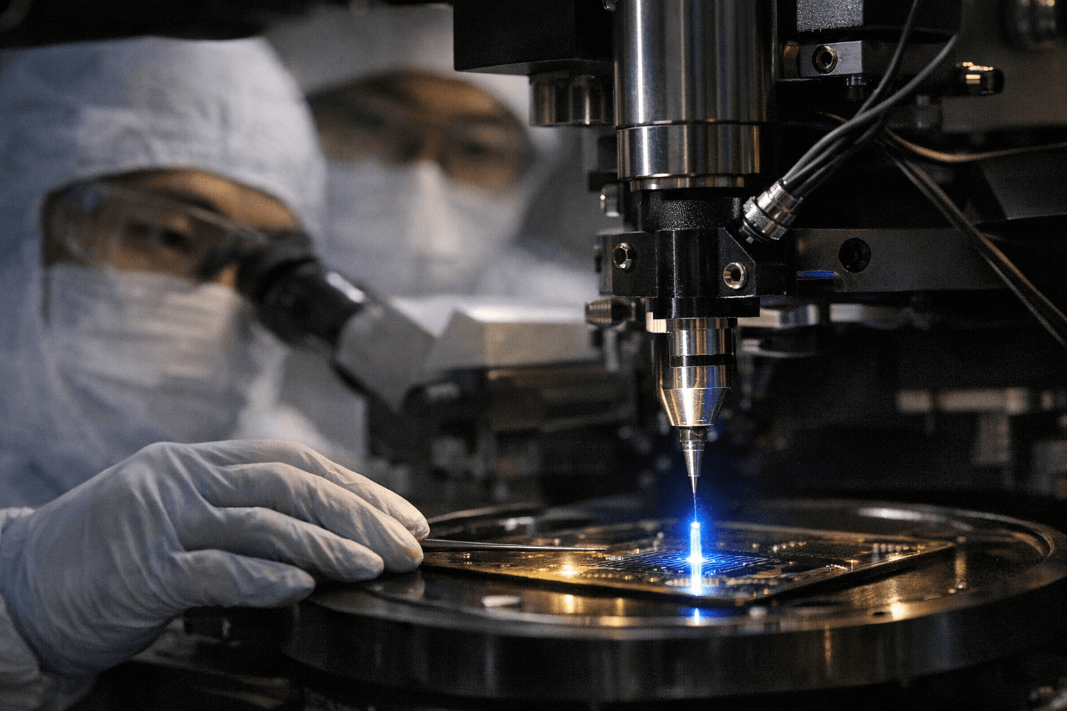
Researchers at KAIST, working with authors from POSTECH, reported a new nano 3D printing technique that fabricates vertical perovskite nanolasers directly on semiconductor chips. The method, called ultra-fine electrohydrodynamic 3D printing, controls attoliter-scale droplets to build pillar-shaped nanostructures with diameters far below the width of a human hair. Combining the printing with gas-phase crystallization control yields near-single-crystalline perovskite material and extremely smooth surfaces, two factors that support efficient lasing.
The vertical geometry of the printed pillars reduces light leakage into the substrate, a common loss channel for conventional horizontal lasers, and delivers improved laser efficiency. Researchers can tune the pillar height to adjust emission color, allowing the team to create patterned areas whose laser wavelengths vary with structure height. Those patterned emissions are difficult to replicate without the same fabrication approach, suggesting immediate anti-counterfeiting applications for secure labeling and product authentication.
The technical advance responds to limits in lithographic fabrication when scaling optical components to higher densities. Lithography often requires multiple steps, planar processing constraints, and complex alignment as device features move into the nanoscale. Direct 3D nanoprinting bypasses many of those constraints by building three-dimensional optical elements where they are needed on the chip, offering a route to flexible, high-density integration that could support ultra-high-speed optical computing and emerging on-chip photonic systems.
For the 3D printing community, the development signals an expansion of additive manufacturing from macroscale tooling and prototypes into functional nanophotonics. The practical value today is primarily strategic: follow material compatibility, process control, and packaging developments as they determine whether the technique moves out of specialized labs and into foundries or service offerings. Expect near-term activity around optimizing crystallization, integrating printed pillars with electrical and cooling infrastructure, and refining repeatability at wafer scale.
Longer term, the method could influence how makers, service bureaus, and small labs approach optical device prototyping. If direct nanoprinting workflows become accessible, you will be able to experiment with on-chip light sources and secure optical tags without resorting to multi-step lithography. For now the advance highlights a clear direction for merging additive manufacturing precision with practical photonic function on silicon.
Sources:
Know something we missed? Have a correction or additional information?
Submit a Tip